 | –≠–ª–µ–∫—Ç—Ä–æ–Ω–Ω—ã–π –∫–æ–º–ø–æ–Ω–µ–Ω—Ç: 111RKI | –°–∫–∞—á–∞—Ç—å:  PDF PDF  ZIP ZIP |

110A
PHASE CONTROL THYRISTORS
Stud Version
111RKI SERIES
Bulletin I25152/B
Features
High current and high surge ratings
dv/dt = 1000V/µs option
Ceramic housing
Threaded studs UNF 1/2 - 20UNF2A
Types up to 1200V V
RRM
/V
DRM
di/dt = 300A/µs
Typical Applications
DC motor controls
Controlled DC power supplies
AC controllers
I
T(AV)
110
A
@ T
C
90
∞C
I
T(RMS)
172
A
I
TSM
@
50Hz
2080
A
@ 60Hz
2180
A
I
2
t
@
50Hz
21.7
KA
2
s
@ 60Hz
19.8
KA
2
s
V
DRM
/V
RRM
400 to 1200
V
t
q
typical
110
µs
T
J
- 40 to 140
∞C
Parameters
111RKI
Units
Major Ratings and Characteristics
case style
TO-209AC (TO-94)
Next Data Sheet
Index
Previous Datasheet
To Order

111RKI Series
2222222222222
12
ELECTRICAL SPECIFICATIONS
Voltage Ratings
Voltage
V
DRM
/V
RRM
, max. repetitive
V
RSM
, maximum non-
I
DRM
/I
RRM
max.
Type number
Code
peak and off-state voltage
repetitive peak voltage
@ T
J
= T
J
max.
V
V
mA
40
400
500
111RKI
80
800
900
20
120
1200
1300
I
T(AV)
Max. average on-state current
110
A
180∞ conduction, half sine wave
@ Case temperature
90
∞C
I
T(RMS)
Max. RMS on-state current
172
DC @ 83∞C case temperature
I
TSM
Max. peak, one-cycle
2080
t = 10ms
No voltage
non-repetitive surge current
2180
A
t = 8.3ms
reapplied
1750
t = 10ms
100% V
RRM
1830
t = 8.3ms
reapplied
Sinusoidal half wave,
I
2
t
Maximum I
2
t for fusing
21.7
t = 10ms
No voltage
Initial T
J
= T
J
max.
19.8
t = 8.3ms
reapplied
15.3
t = 10ms
100% V
RRM
14.0
t = 8.3ms
reapplied
I
2
t
Maximum I
2
t for fusing
217
KA
2
s
t = 0.1 to 10ms, no voltage reapplied
V
T(TO)1
Low level value of threshold
voltage
V
T(TO)
2
High level value of threshold
voltage
r
t1
Low level value of on-state
slope resistance
r
t2
High level value of on-state
slope resistance
V
TM
Max. on-state voltage
1.57
V
I
pk
= 350A, T
J
= T
J
max., t
p
= 10ms sine pulse
I
H
Maximum holding current
150
I
L
Typical latching current
400
0.82
(16.7% x
x I
T(AV)
< I <
x I
T(AV)
), T
J
= T
J
max.
2.16
(16.7% x
x I
T(AV)
< I <
x I
T(AV)
), T
J
= T
J
max.
1.70
(I >
x I
T(AV)
),T
J
= T
J
max.
Parameter
111RKI
Units Conditions
1.02
(I >
x I
T(AV)
),T
J
= T
J
max.
On-state Conduction
KA
2
s
V
m
mA
T
J
= 25∞C, anode supply 6V resistive load
di/dt
Max. non-repetitive rate of rise
Gate drive 20V, 20
, t
r
1µs
of turned-on current
T
J
= T
J
max, anode voltage
80% V
DRM
Gate current 1A, di
g
/dt = 1A/µs
V
d
= 0.67% V
DRM
,
T
J
= 25∞C
I
TM
= 50A, T
J
= T
J
max., di/dt
= -5A/µs, V
R
= 50V
dv/dt
= 20V/µs, Gate 0V 25
Parameter
111RKI
Units Conditions
t
d
Typical delay time
1
Switching
t
q
Typical turn-off time
110
µs
300
A/µs
Next Data Sheet
Index
Previous Datasheet
To Order

111RKI Series
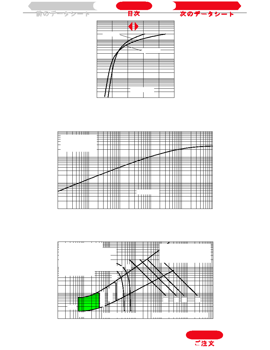
Fig. 5 - Maximum Non-Repetitive Surge Current
Fig. 6 - Maximum Non-Repetitive Surge Current
Fig. 4 - On-state Power Loss Characteristics
Fig. 3 - On-state Power Loss Characteristics
To Order
Next Data Sheet
Index
Previous Datasheet
111RKI Series
Fig. 9 - Gate Characteristics
Fig. 8 - Thermal Impedance Z
thJC
Characteristic
Fig. 7 - On-state Voltage Drop Characteristics
To Order
Next Data Sheet
Index
Previous Datasheet

111RKI Series
23
dv/dt
Maximum critical rate of rise of
off-state voltage
I
RRM
Max. peak reverse and off-state
I
DRM
leakage current
Blocking
500
V/µs
T
J
= T
J
max. linear to 80% rated V
DRM
Parameter
111RKI
Units Conditions
20
mA
T
J
= T
J
max, rated V
DRM
/V
RRM
applied
P
GM
Maximum peak gate power
12
T
J
= T
J
max, t
p
5ms
P
G(AV)
Maximum average gate power
3.0
T
J
= T
J
max, f = 50Hz, d% = 50
I
GM
Max. peak positive gate current
3.0
A
T
J
= T
J
max, t
p
5ms
+V
GM
Maximum peak positive
gate voltage
-V
GM
Maximum peak negative
gate voltage
I
GT
DC gate current required
T
J
= - 40∞C
to trigger
mA
T
J
= 25∞C
T
J
= 140∞C
V
GT
DC gate voltage required
T
J
= - 40∞C
to trigger
V
T
J
= 25∞C
T
J
= 140∞C
I
GD
DC gate current not to trigger
6.0
mA
Parameter
111RKI
Units Conditions
20
10
Triggering
T
J
= T
J
max
TYP.
MAX.
180
-
80
100
40
-
2.5
-
1.6
2
1
-
Max. gate current/ voltage not to
trigger is the max. value which
will not trigger any unit with rated
V
DRM
anode-to-cathode applied
Max. required gate trigger/ cur-
rent/ voltage are the lowest value
which will trigger all units 12V
anode-to-cathode applied
W
V
T
J
= T
J
max, t
p
5ms
T
J
Max. operating temperature range
-40 to 140
T
stg
Max. storage temperature range
-40 to 150
R
thJC
Max. thermal resistance,
junction to case
R
thCS
Max. thermal resistance,
case to heatsink
T
Mounting torque, ± 10%
15.5
Non lubricated threads
(137)
14
Lubricated threads
(120)
wt
Approximate weight
130
g
Parameter
111RKI
Units
Conditions
0.27
DC operation
0.1
Mounting surface, smooth, flat and greased
Thermal and Mechanical Specification
∞C
K/W
Nm
(lbf-in)
Case style
TO - 209AC (TO-94)
See Outline Table
V
GD
DC gate voltage not to trigger
0.25
V
To Order
Next Data Sheet
Index
Previous Datasheet